artificial intelligence
connections

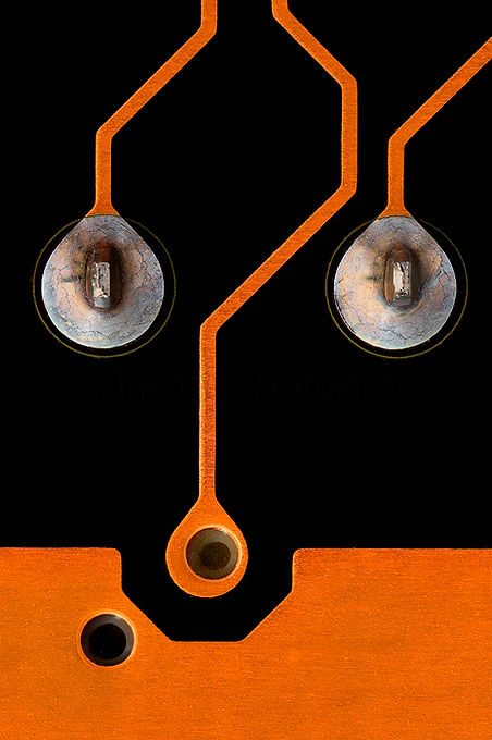
connections #1 (e-face), 2012
field view size: 0.25 x 0.17 in
print: 52 x 34.6 in / 25.9 x 17.3 in
e-face
The Digital Age
electron
contact
connections
web of connections
conductive material
conductive tracks
plated-through holes
printed circuit
electronic circuit
surface-mount technology
through-hole technology
electronics
electronics engineering

connections #2 (new paths 1), 2012
field view size: 0.30 x 0.45 in
print: 34.6 x 52 in / 17.3 x 25.9 in
paths
roads
electron
contact
connections
web of connections
conductive material
conductive tracks
plated-through holes
printed circuit
electronic circuit
surface-mount technology
through-hole technology
electronics
electronics engineering

connections #3 (orange landscape 1), 2012
field view size: 0.27 x 0.18 in
print: 52 x 34.6 in / 25.9 x 17.3 in
landscape
orange
e-fingers
electron
contact
connections
web of connections
conductive material
conductive tracks
plated-through holes
printed circuit
electronic circuit
surface-mount technology
through-hole technology
electronics
electronics engineering

connections #4 (orange landscape 2), 2012
field view size: 0.12 x 0.18 in
print: 34.6 x 52 in / 17.3 x 25.9 in
landscape
orange
e-fingers
electron
contact
connections
web of connections
conductive material
conductive tracks
plated-through holes
printed circuit
electronic circuit
surface-mount technology
through-hole technology
electronics
electronics engineering

connections #5 (orange landscape 3), 2012
field view size: 0.42 x 0.28 in
print: 52 x 34.6 in / 25.9 x 17.3 in
landscape
orange
electron
contact
connections
web of connections
conductive material
conductive tracks
plated-through holes
printed circuit
electronic circuit
surface-mount technology
through-hole technology
electronics
electronics engineering
connections
Connecting tracks, contact pads, and conductive pathways allow electrons to move a near-light speeds. Like electronic neurotransmitters, they transfer valuable information from one neural location to another, and keep several components in touch so that their function can be performed.
Basic constituents of communication networks, sometimes simple and sometimes complex, these integrated elements fit surprisingly well in the physical dimensions of the supporting board.
The optimization of space is precisely what generates these suggestive geometries: straight and broken lines, sometimes ending at a connection point with another pathway. Their sober chromatic range is extremely expressive.
Faces and eyes sculpted by a robot, a portrait of science. Tracks and contacts wriggling through tiny spaces, rising, gyrating, and ducking like elegant sculptures.
Machines, with their robotic arms, perform the precision work required to design and print the endless connection networks of most electronic devices.
The artificial microlandscapes resulting from human design and robotic manufacture display traces of their mixed parentage.
Antonio Romero
electron,
contact,
connections,
web of connections,
conductive material,
conductive tracks,
plated-through holes,
printed circuit,
electronic circuit,
surface-mount technology,
through-hole technology,
electronics,
electronics engineering
The caption of each work are displayed on the pdf (artificial_intelligence_a_romero_2017.pdf) of this project. Please email me for further information.